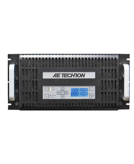
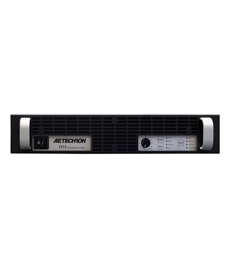
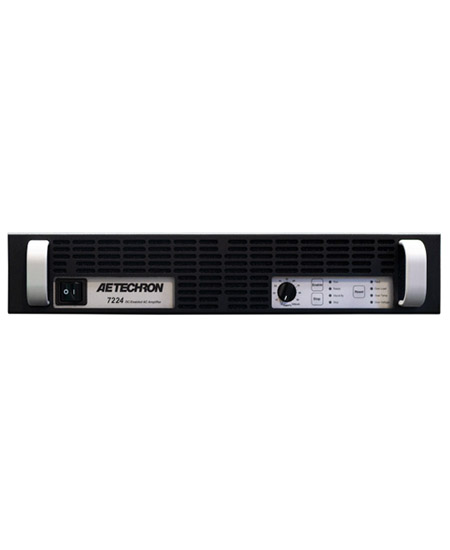
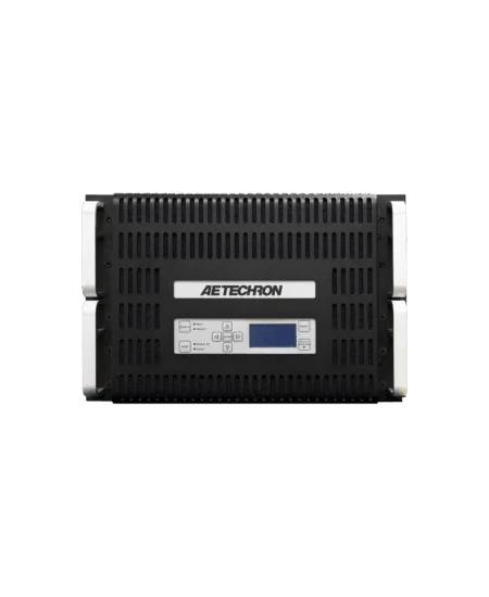
The 7224 Linear Amplifier delivers power, speed, and precision in a compact 2U form factor. Designed for lab, test, and simulation environments, it provides outstanding performance for demanding applications.
Key Features:
- Up to 900W RMS output power
- Operates in controlled-current or controlled-voltage mode
- Field-configurable for low or high impedance loads
- DC to 1 MHz small signal bandwidth
- Produces up to 50A current or 158V peak
- Slew rate of 90 V/μs for sharp waveform reproduction
- Over-voltage, over-current, and over-temp protection circuits
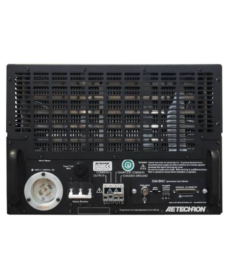
- Compact 2U rack-mount or benchtop design
- Suitable for Helmholtz coil drivers, MRI/NMR, SMPS component testing
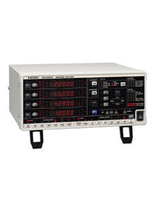 Hioki POWER METER PW3337