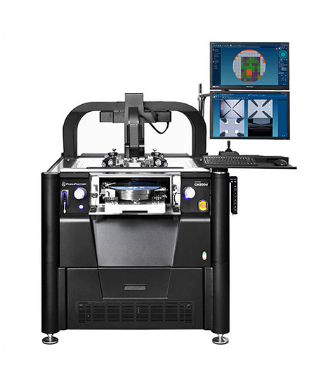
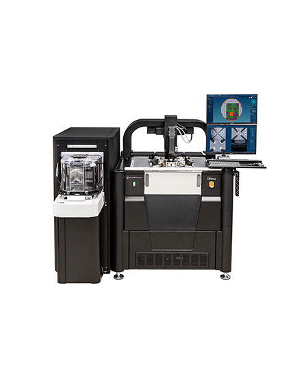
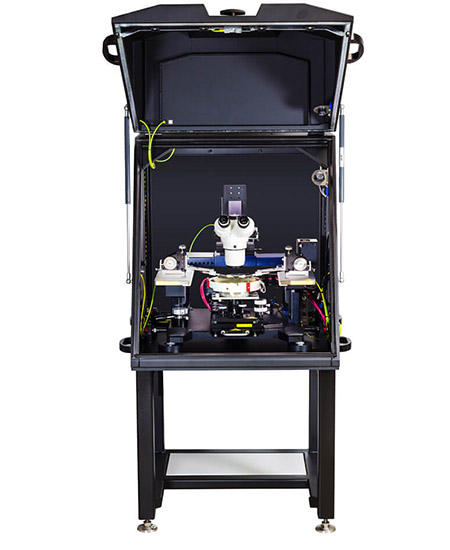
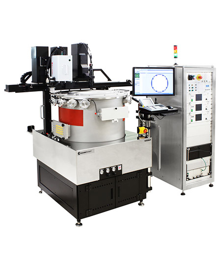
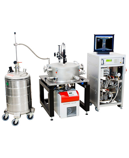
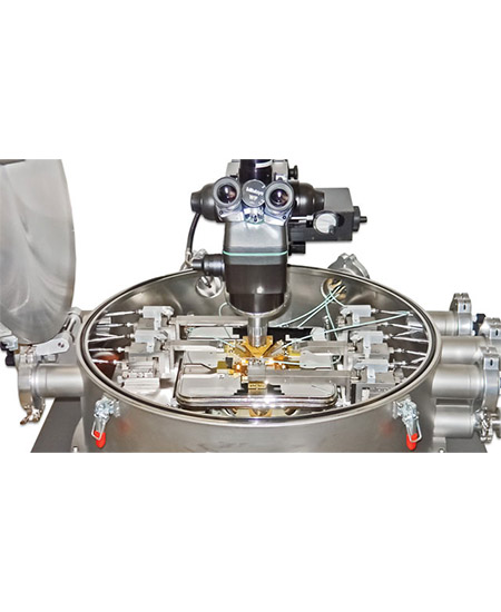
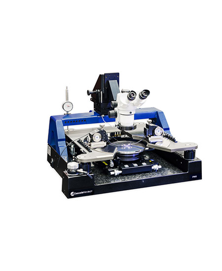
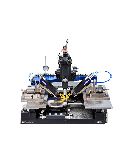
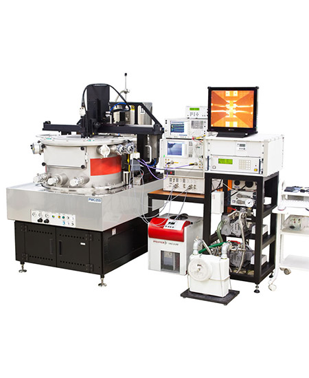
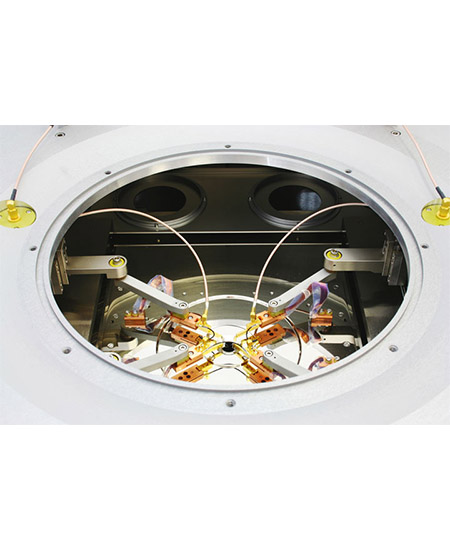
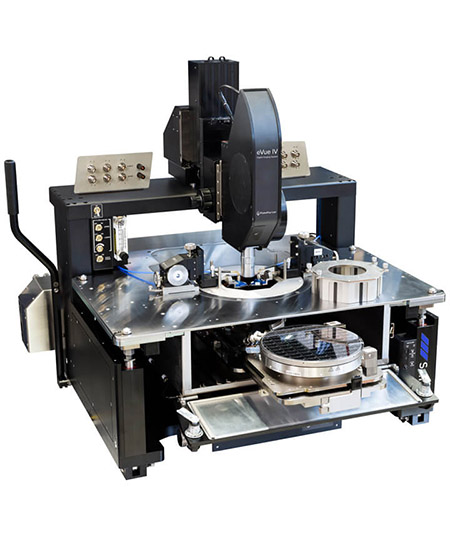
The Cascade PLC50 is a precise, cost-effective cryogenic wafer probing system designed for research labs. It enables testing down to 77 K with liquid nitrogen or below 7 K with liquid helium, supporting DC, RF, MEMS, and optoelectronic measurements.
Key Features:
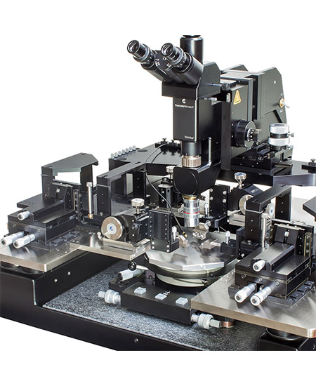
- Compatible with wafers up to 100 mm and single dies.
- Operates at 77 K (LN₂) or < 7 K (LHe).
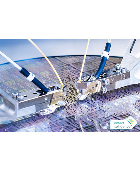
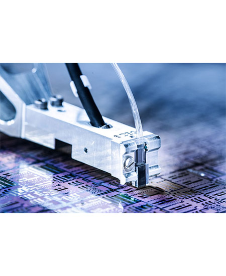
- Up to six positioners for flexible probing.
- Independently cooled cold shield ensures stable, accurate results.
- Ice- and condensation-free probing in vacuum conditions.
- Ergonomic design with hinged lid and easy microscope access.
- Independent chuck stage and positioner control for high throughput.