Description
Overview of EPS150TESLA Probe Station
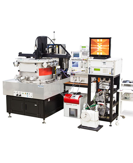
The Cascade EPS150TESLA is a manual 150 mm on-wafer power device characterization system designed to energize high-power semiconductor measurements with accuracy, safety, and reliability. Built for research labs and device engineers, it provides a versatile platform to measure breakdown voltages up to 3,000 V, with optional coaxial upgrades reaching 10,000 V, and supports high-current probing up to 100 A.
Its shielded environment ensures noise reduction and operator safety, while advanced grounding and arcing protection minimize risks during sensitive high-voltage tests. Whether characterizing silicon, SiC, or GaN devices, the EPS150TESLA allows engineers to collect precise and repeatable data across multiple conditions.
Optimized High Power Measurement Setup
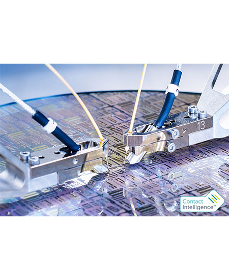
The system integrates seamlessly with leading analyzers using a multi-purpose SIGMA instrument integration kit, offering shorter cabling, a universal chuck connection, and an optimized signal path. Triax probes with protected guards and safe probe tip exchange capabilities provide confidence during delicate, high-voltage probing tasks.
Advanced High Power Chuck Design
The triaxial chuck is designed for low-leakage, high-voltage operation up to 3 kV, with an optional coaxial upgrade for 10 kV. Special surface coatings ensure stable contact, while thin-wafer handling capabilities make it suitable for next-generation device technologies. High-current operation up to 100 A with minimal resistance ensures accurate Rds(on) and breakdown testing.
Safe and Reliable Operation
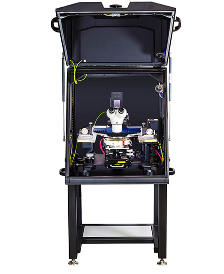
Safety is integral to the EPS150TESLA. Features include a shield enclosure with interlock, arcing protection, and a comprehensive grounding system for both operator and device safety. The EMI and light-tight shielded environment ensures clean signals with reduced measurement noise, enhancing repeatability and accuracy.
Applications of EPS150TESLA
- Power semiconductor device characterization (Si, SiC, GaN).
- Breakdown voltage and Rds(on) measurements.
- High-current device evaluation up to 100 A.
- Research and development in power electronics.
- Thin-wafer handling for next-gen technologies.
Technical Specifications Table
| Feature | Specification |
| Wafer Size | 150 mm |
| Voltage Range | Up to 3,000 V triaxial (optional 10,000 V coaxial) |
| Current Range | Up to 100 A |
| Chuck Design | Triaxial with low-leakage coating |
| Environment | EMI / light-tight shielded enclosure |
| Safety Features | Interlock system, arcing protection, advanced grounding |
| Integration | SIGMA kit for analyzer connection, optimized signal path |
| Temperature Handling | Thin wafer capability |
Click here to learn more about similar products from FormFactor Beaverton Inc.