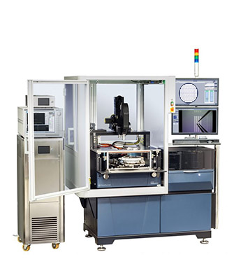
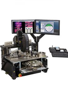
Description
Cascade TESLA200 automated wafer power device characterization
`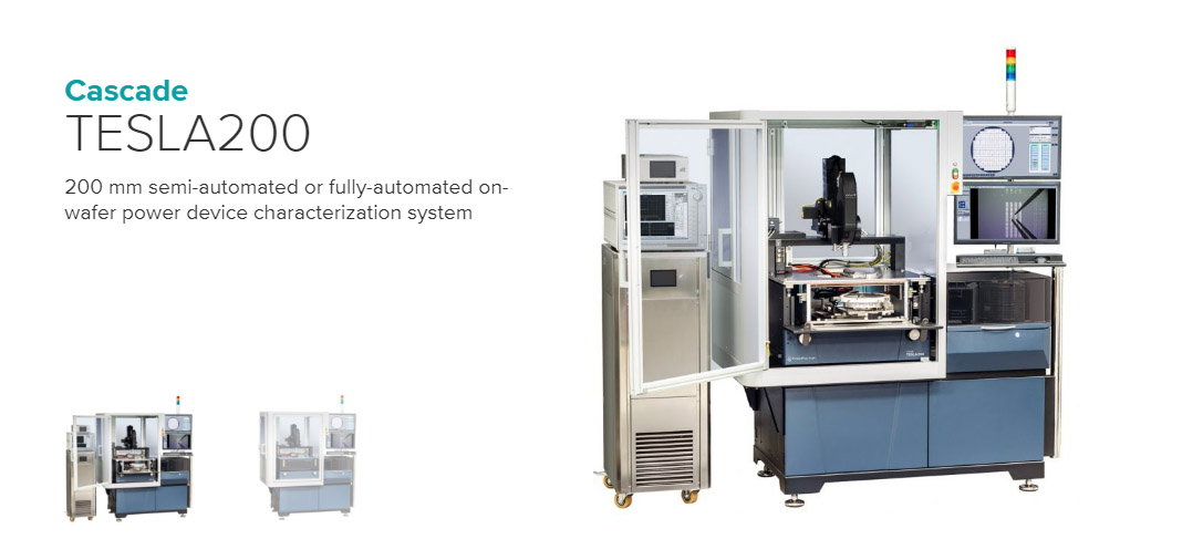
TESLA200 Overview
Designed specifically for IGBT/power MOSFET (GaN, SiC, Si) device measurements at the wafer level, the new TESLA200 on-wafer power semiconductor probing system is engineered to provide accurate data up to 3, kV (triaxial) / 10 kV (coaxial) and 200 A (standard) / 600 A (high current). With next generation test capabilities, anti-arcing solutions, wafer automation, and support for both engineering probes and production probe cards, the TESLA200 now enables complete thermal testing (-55°C to 300 °C) with fully-automatic thinned/warped/TAIKO wafer loading. One system covers all on-wafer high power test needs, from R&D to niche production.
Applications: High Power
TESLA200 Key Features
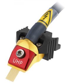
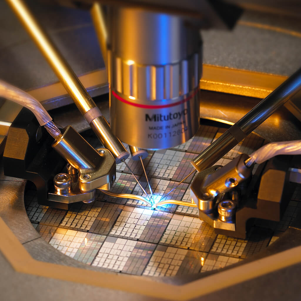
High-voltage/current Probes
 |
|
- On-wafer power device characterization up to 10,000 V DC / 600 A
- Reduced probe and device destruction at high currents up to 20 A DC and 300 A pulse
- Increased isolation resistance and dielectric strength to provide full triaxial capability at high voltage (3,000 V) for low-leakage measurement
|
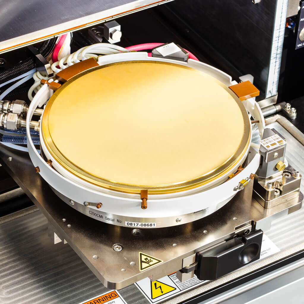
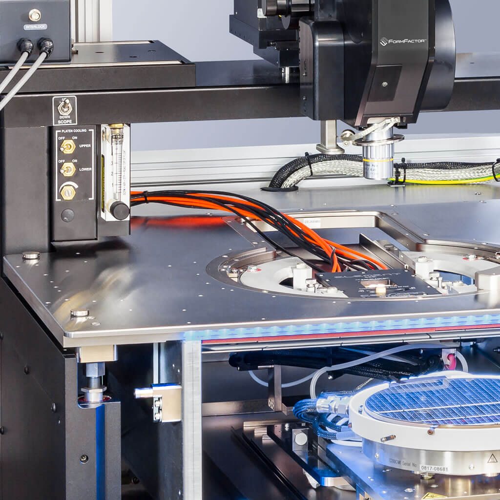
Gold-plated TESLA High-power MicroVac™ Chucks
- Prevent thin wafers from curling and breaking
- Advanced MicroVac chuck surface for minimum contact resistance between wafer and chuck
- Accurate Rds(on) measurement at high current
- Accurate UIS measurements at high temperature
|
|
 |
 |
|
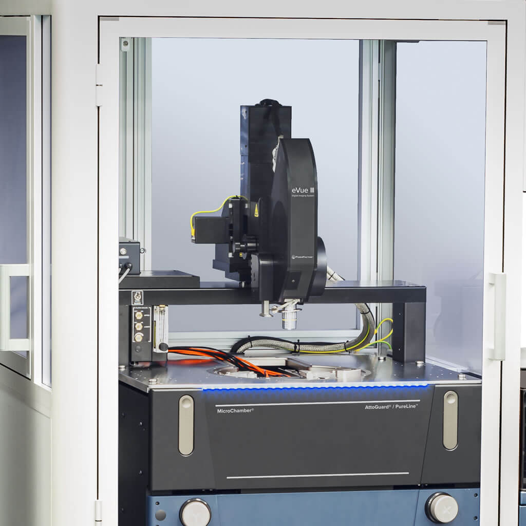
Safety for Operator
- Safety interlock system with clear enclosure for operator safety during device measurements
- Roll-out stage for full wafer access and easy wafer loading/unloading
|
Seamless Integration
- Convenient connection kits for easy and safe system integration with power device analyzers from Keysight Technologies and major suppliers
- Seamless integration between Velox and analyzers/measurement software
|
|
 |
 |
|
Productivity
- High-throughput wafer autoloading (standard, thinned, warped, TAIKO)
- Contact Intelligence enables higher yield, accurate Rds vertical device measurements over temperature automatically
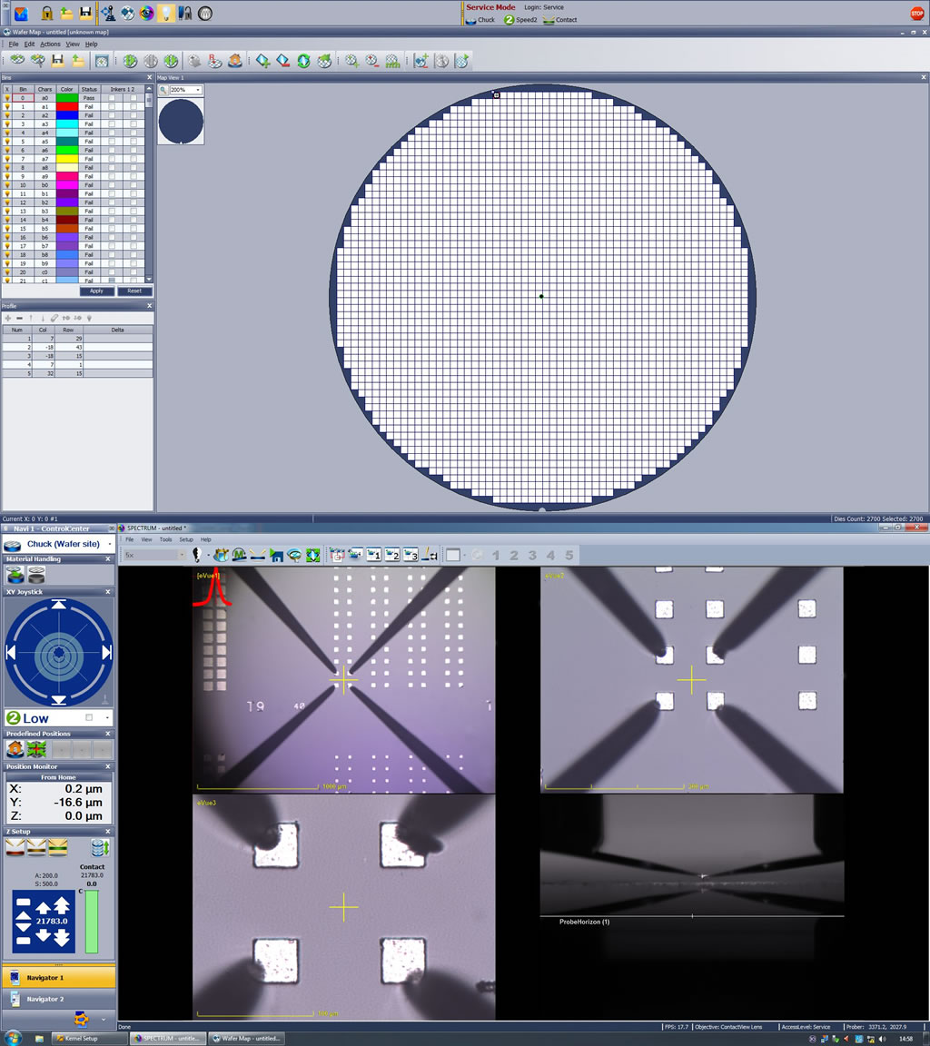
- Easy on-screen navigation, wafer mapping, and operation of accessories with Velox
|
|
Cascade TESLA200 automated wafer power device characterization.