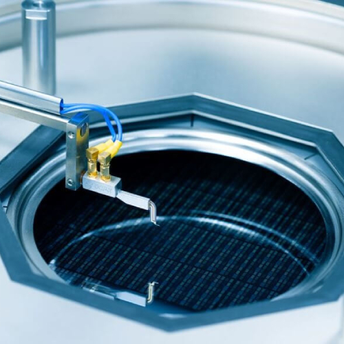
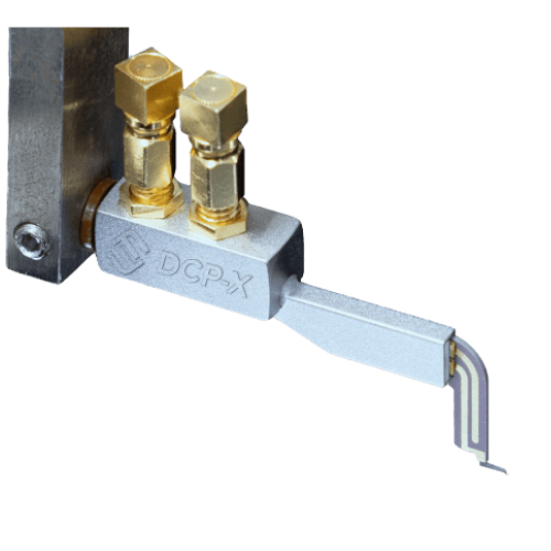
Description
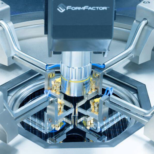
The new DCP-X probe is designed for Device characterization, R&D, and Test Services Engineers, and Scientists, who need to perform highest accuracy and repeatable on-wafer device electrical measurements (IV, CV, LFN) for device characterization and modelling, and general DC testing on small pads.
The DCP-X probe with MEMs technology measures existing and leading-edge (2, 3, 5 nm) devices error-free, on all pad materials, micro-bumps, & slotted pads down to 20 μm size, virtually eliminating “re-testing” due to poor contact, and with little to no cleaning, over the full thermal range with significantly lower CoT (cost of test).
Traditional DC probes using single cantilever tungsten needles have high series resistance (probe and pad
Rc) causing inaccurate data, damage pads with heavy overdrive/skating, and require frequent cleaning. But the new Formfactor DCP-X probe with “World’s First” true- kelvin, guarding & advanced MEMs contacting technology, delivers revolutionary performance with 1000x lower probe Rc, 0.15% error on 2Ω RDS device, low skate, and long lifetime >500K contacts.
Features & Benefits of DCP-X Probe:
Eliminate errors:
- Virtually error-free (0.15% on 2Ω RDS device) vs typical wafer process 0.3% variation
- High accuracy with no misleading test data
- 1000x lower probe contact resistance (1-5 mΩ)
- Low leakage fA guard plane (force/sense)
Reduce pad damage:
- Small scrub (7μm) with only 20μm overdrive
- Minimal pad damage with optimized micro-scrub
- Small 6um tip size, and 20μm pitch (Kelvin version)
Probe smaller:
- Advanced MEMs tip with a ruggedized design
- Probe all pad materials & slotted pads without tip deformation
- Probe micro bumps down to ~50 μm
- Supports temperatures from -55°C to 175°C
Save time:
- Quick probe setup using standard probe mount
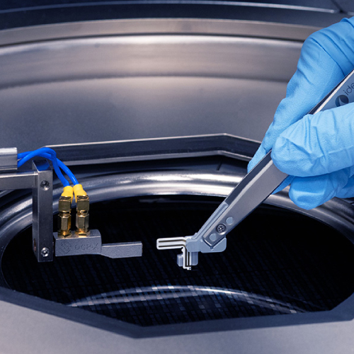
- Easy probe tip replacement in prober with a special tool
- Reduced tip damage/contamination
- Use with manual or motorized positioners
- Optimized for fast testing with Autonomous DC probing
Lower costs:
- Production level quality in engineering probe
- Replaceable blade/tip design
- Long lifetime with >500,000 touchdowns (Kelvin version)
- 98% cost reduction (tips) compared to DCP-HTR
Test faster:
- Less time cleaning with low scrub MEMs tip minimizes debris
- Minimum to no cleaning with Kelvin tip
- Low cleaning with Single (Quasi-kelvin) tip

 |
 |