Description
|Z| Probe® PCB Overview
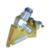
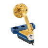
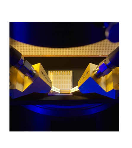
Flexibility is the key for efficient PCB and ceramic testing. The |Z| Probe® PCB is simple to align and handle and can be easily positioned. It optimally replaces costly test fixtures which are often inflexible. A robust design makes the |Z| Probe PCB easy to handle and offers a long working life typically more than one million (1,000,000) contacts.
The planar tip of the |Z| Probe PCB has precisely calculated, parallel, separate contact springs which move independently of one another, allowing a precise, quick and simple contact with the DUT, even if there are significant contact height differences. This unique feature as well as the overall very robust design of the |Z| Probe PCB ensures a long life and simple handling.
Used in conjunction with a manual probe system including probe positioners and calibration substrates, the |Z| Probe PCB becomes the ultimate tool for all RF circuit probing needs.
|Z| Probe® PCB Key Features
- Replace costly and inflexible test fixtures with easy-to-use probe tips
- Long lifetime – typically over 1,000,000 contacts
- GS/SG footprint up to 4 GHz and GSG up to 20 GHz
- High-power RF test: up to 30 Watts
- Test at temperatures from -60°C to 200°C

