1 800 665 7301 | info@tmetrix.com

FormFactor Beaverton Inc

Showing 1–16 of 69 results


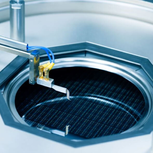
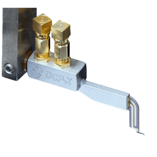
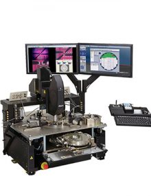
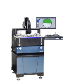
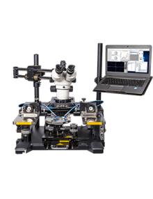
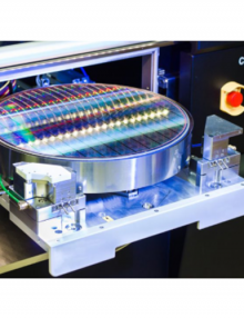
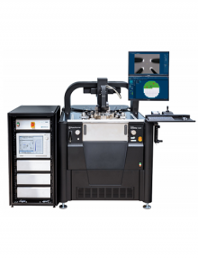
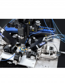
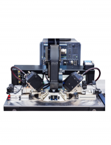
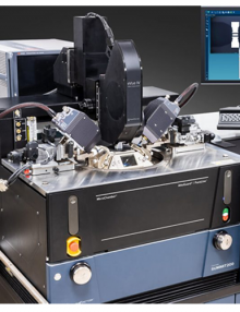
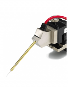
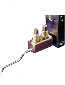
  • The DCP-X probe is designed for engineers and scientists in device characterization, R&D, and testing, offering highly accurate and repeatable on-wafer electrical measurements (IV, CV, LFN). It uses MEMS technology to measure advanced devices (2, 3, 5 nm) on various pad materials, micro-bumps, and pads as small as 20 μm, reducing the need for retesting and cleaning while covering the full thermal range at lower testing costs. Compared to traditional probes, the DCP-X provides 1000x lower contact resistance, minimal skate, and over 500,000 contact cycles, ensuring precise measurements and longer probe life.

  • The TESLA300 Advanced On-Wafer Power Semiconductor Probe System is an integrated high-power test solution that enables the collection of accurate high-voltage and high-current measurement data up to 3 kV (triaxial) / 10 kV (coaxial) and 200 A (standard) / 600 A (high current), with complete operator safety.

    • Vector Network Analyzer (option up to 26.5GHz)
    • WinCal XE calibration software
    • Uses best measurement practices for optimized measurements
    • Known measurement accuracy traced back to independent standards
    • Supported by the measurement experts to make you successful
    • Best in class RF performance
    • Small benchtop footprint
    • Industry standard calibration techniques
    • Extended 2 Year warranty on FormFactor products for educational customers


    • Re-configurable for DC, RF, mmW, FA, WLR and more
    • table and repeatable measurements over a wide thermal range
    • Moisture-free, light-tight and EMI-shielded test environment with MicroChamber® technology
    • Minimize AC and spectral noise
    • Manual 3-axis stage with ergonomic controls
    • Fast, accurate “hands on” wafer positioning
    • Quick, safe, and comfortable wafer access


    • Comfortable and ergonomic operation
    • Thermal range ambient to +300°C
    • RF/microwave device characterization, FA and design debug
    • Seamless integration between Velox and analyzers/measurement software
    • Complete solutions using probe positioners and probe cards
    • Achieve unsurpassed RF/mmW measurement and calibration accuracy with integrated RF tools and WinCal
    • Shortest signal path test integration for accurate, thermally stable, and low-error data collection
    • Powerful automation tools, reduce total test time on wafers, singulated dies, and modules
    • Faster time to first data for standard and “hard to test” devices such as thin wafer, small pad and high power
    • Advanced 4-axis semi-automatic stage for accurate positioning and repeatable probe-to-pad contact


  • Genius Education Kits Overview


    • Flexibility
      • Temperatures range from -60°C to +300°C
      • Surfaces are nickel or gold-plated
      • Hybrid chuck design – operation with and without cooling unit
      • Field-upgradeable: On-site cold upgrades for all main prober platforms
    • Highest Efficiency for Reduced Cost of Test
      • Up to 25% lower air consumption (CDA) than other systems on the market with no compromise in transition times
      • Up to 15% faster transition times than other systems on the market
    • Low Thermal Resistance
      • Low Thermal Resistance Technology
      • MultiSense with multiple temperature sensors
      • Best temperature accuracy and uniformity
    • Superior Electrical Performance
      • Isolated from ground
      • Includes a jack for grounding and biasing
      • Highly planar chuck surface for consistant contact force and overtravel


  • PureLine 3 Technology

    First automated probe station to achieve -190dB spectral noise*

    Plug In and Go

    Integrated TestCell Power Management provides fully managed and filtered AC power to the entire system, prober and instruments

    Autonomous 24/7 Operation

    Up to 4x faster flicker noise thermal testing on 30 μm pads

    Reduce Setup Time and Costs
    Exclusive low noise site survey, and system verification services


    • Quick and easy probe tip navigation
    • Maximizes field-of-view
    • High magnification
    • Shadow-free view of the corresponding features
    • Automatically configure and optimize performance
    • cTUVus certified and CE
    • Compatible with TopHat for perfect shielding
    • 24/7 operating, Increased MTBF
    • Stops all system motion and warns of unobserved contact


  •  

    Contact Intelligence

    • Ease of use –  Less experienced operators can perform DC measurements by simply pushing a button. This reduces the need of experienced users full time on each system.
    • Reduced Soak Time – The system will automatically re-align the probes to the pads if they drift from alignment. This reduces test time and increases throughput.
    • Unattended Use – Measurements can be left running over night or the weekend, testing all devices on the wafer, and at different temperatures without the need of an operator.


    • Highest accuracy with backlash-free positioning
    • Drift-free measurements over temperature and time*
    • Easy, and safe swapping between arms
    • Best signal integrity using optimized probe cabling systems
    • Full thermal capability*
    • Manual or progammable


    • Ease of use –  Less experienced operators can perform an RF calibration up to 330 GHz by simply pushing a button. This reduces the need of experienced users full time on each system.
    • Reduced Soak Time – The system will automatically re-align the probes to the pads if they drift from alignment. This reduces test time and increases throughput.
    • Unattended Use – Measurements can be left running over night or the weekend, testing all devices on the wafer, and at different temperatures without the need of an operator.
    • Calibration Monitor and Re-calibration – System will continuously monitor calibration drift, and automatically re-calibrate the system should the drift exceed a predefined limit.


    • Comprehensive,
    • Turn-key Integrated Measurement System (IMS)
    • with Keysight PNA for On-wafer R&D Measurements
    • from RF to millimeter wave to Terahertz


  • Accurate and precise measurement of device parameters up to 3,000 V

    • Coaxial and triaxial measurements up to 3,000 V
    • High-quality construction with low-noise electrical performance
    • Replaceable probe tips in a variety of tip sizes
    • Temperature range of -55 to 300ºC
    • Triaxial measurement ensures a much better understanding of device leakage in the off state
    • Highly reliable, stable and repeatable measurements
    • Integrally designed as part of a complete measurement solution


  • Delivers superior guarding and shielding

    • High-quality construction with low-noise electrical performance
    • Kelvin version for convenient 4-point measurements
    • Replaceable coaxial probe tips, with choice of tip radii, and full electrical guard to the probe tip
    • SSMC 50 connectors
    • Ultra-low, fA and fF measurements from -65 º C to 150 º C


    • Light-tight version and EMI-shielded version for low noise and light-sensitive measurements
    • Application flexibility, ideal for use in high frequency applications
    • Sized to accommodate thermal chucks, laser cutter, and video equipment on the probe system
    • Suitable for integration with vibration isolating tables


Showing 1–16 of 69 results

Filters


Technologies

Latest News