Discount Products: Look through products available for a 25% – 50% discount in 2020. The items provided on a first come, first serve basis. View Discounted Products
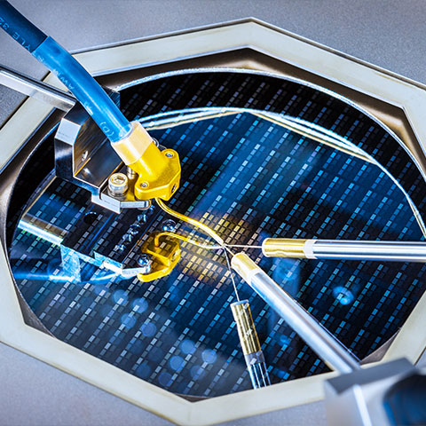
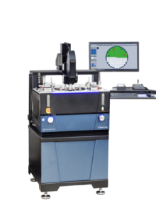
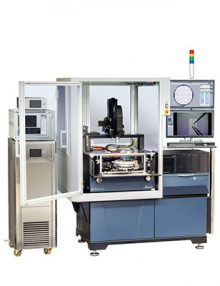
The TESLA300 Advanced On-Wafer Power Semiconductor Probe System is an integrated high-power test solution that enables the collection of accurate high-voltage and high-current measurement data up to 3 kV (triaxial) / 10 kV (coaxial) and 200 A (standard) / 600 A (high current), with complete operator safety.
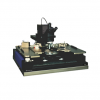
Introducing the TESLA300 On-Wafer Power Semiconductor
The TESLA300 provides lab automation capabilities and enables high-power electrical measurements for device characterization, high-volume engineering and highly challenging applications. It is also ideally suited to customized solutions, niche production applications, and emerging markets.
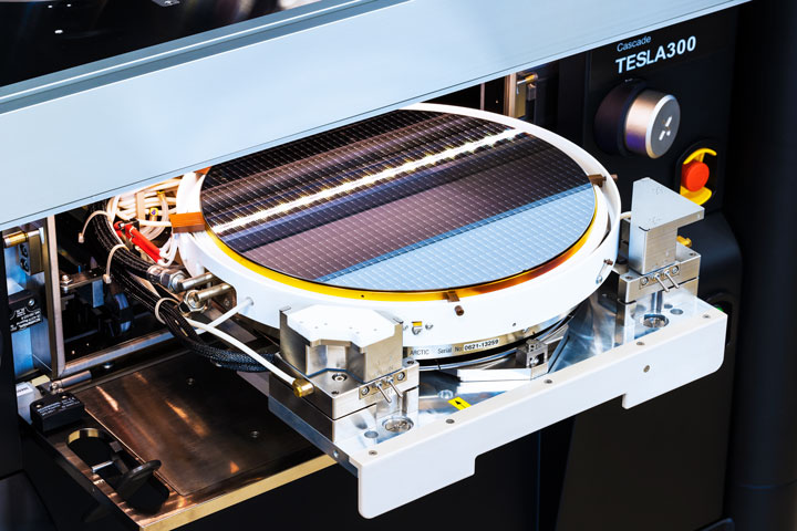
Patented AttoGuard technology built in TESLA300 significantly improves low-leakage and low-capacitance measurements. In combination with FormFactor’s patented TESLA FemtoGuard™ thermal chuck technology, the TESLA300 provides a fully guarded and shielded test environment. The high-power TESLA FemtoGuard chuck also incorporates MicroVac™ technology enabling low-contact resistance, thin wafer handling and maximum power dissipation.
Key Features
Gold-plated TESLA High-power MicroVac™ Chucks:
Prevent thin wafers from curling and breaking
Advanced MicroVac chuck surface for minimum contact resistance between wafer and chuck
Accurate Rds(on) measurement at high current
Accurate UIS measurements at high temperature
TUV-certified probing environment:
Safety-rated interlock system for high-power testing (meets EN 60947-5-1, EN 60204-1)
Front, side and rear opening doors for ergonomic test setup and operation
Side panel with cable pass-through for easy equipment configuration
Full enclosure design (no light curtain) prevents accidentally tripping the safety interlock and stopping the test
Top-lift wafer loading:
Eliminates lift-pins from chuck for best-in-class power device measurements
Provides the lowest contact resistance from the wafer to the chuck
Supports fully automated testing up to 10kV by eliminating arcing point
Superior performance for vertical device measurements (no lift pin holes under device)
Rollout stage with quick access to auxiliary sites:
Full wafer access via locking roll-out stage
Two patented auxiliary chucks
Auxiliary chucks: High voltage 10 kV compatible multi-purpose mounts for substrates (cleaning, contact)
Automated probe cleaning capabilities
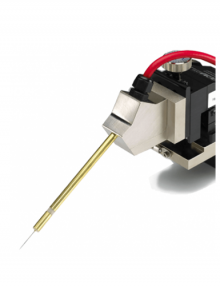
High-voltage/current Probes:
On-wafer power device characterization up to 10,000 V DC / 600 A
Reduced probe and device destruction at high currents up to 20 A DC and 300 A pulse
Increased isolation resistance and dielectric strength to provide full triaxial capability at high voltage (3,000 V) for low-leakage measurement
Connection panels:
Coaxial, triaxial, and pin jack feed troughs are available
Limit cable strain and motion for measurement stability
Instrument stays connected to the back of the panel
Probe connection made at the front of a panel
Simple to re-arrange cabling when needed
Seamless Integration:
Convenient instrument connection kits
Seamless integration between Velox and analyzers/measurement software
Easy and safe system integration with Keysight and Keithley power device analyzers
3D Manual Controls:
Virtual Platen Lift and XY knobs at the front
Intuitive, and precise movement of the chuck in X, Y, and Z-direction
Platen Lift enables an extremely rapid and intuitive way of performing many alignment tasks like setting up the contact height
Material Handling Unit (MHU301):
For fast handling of 200/300 mm wafers
Load/unload wafer to hot/cold chuck (-60° C to +300° C)
Integrated pre-aligner for flat/notch detection
Barcode/2D Matrix code/OCR wafer code recognition from both sides (option)
Quick Access Port option for higher throughput and additional wafer storage
SEMI-compliant load port for up to 25 wafers
For FOUP and FOSB 300 mm wafer cassettes
Thermal Measurements:
Wide range of extremely performant, reliable thermal chuck systems from ATT
Flexibility from hot only to full thermal range of -60°C to +300°C
Up to 25% lower air consumption (CDA) than other systems in the market (300l/min) with no compromise in transition times
Up to 15% faster transition times than other systems in the market
Patented MicroVac™ and FemtoGuard™ Technologies, providing ultra-low noise measurements and controlled leakage, the low residual capacitance for repeatability and advanced measurement accuracy and speed
Field-upgradeable: grows with your needs
Remote operation from home or anywhere in the world:
Safely and easily place probes down in contact with the test pads (full capability with motorized positioners)
Safely move the wafer to different test sites
View and manage live microscope viewing of the probes and the wafer
View Wafer Map test plans
Initiate remote test programs to gather and analyze test data
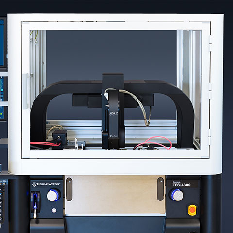
Velox Probe Station Control Software:
User-centred design minimizes training costs and enhances efficiency
Windows 10 compatibility enables the highest performance and safe operation with state-of-the-art hardware
Comprehensive alignment functions – from simple wafer alignment and mapping to advanced probe-to-pad alignment over multiple temperatures for autonomous semiconductor test
Simplified operation for inexperienced users: Reduced training costs with Workflow Guide and condensed graphical user interface
VeloxPro option: SEMI E95-compliant test executive software that enables simplified and safe automation of the entire wafer test cycle
Key Benefits
Scalable from semi-automated operation to the fully-automated prober
Superior high-voltage and high-current measurements
Safe and accurate hands-off testing with reliable and repeatable contact
Contact Intelligence enables unattended tests on small pads
Thermally-induced drift can be automatically corrected, enabling automated temperature transitions over the full temperature range using VueTrack (the effective temperature range and minimum obtainable pad size depend on the probe card and probe card holder or positioner used)
Fast delivery of a wide variety of precise model parameters to enhance the process and device development
Power semiconductor device characterization, DC/RF device characterization, WLR
The full thermal range of -60°C to +300°C, supported by a high thermal stability design
Usage of manual positioners and probe cards within an EMI-shielded environment
Trust the Experts at ACA TMetrix Inc.
ACA TMetrix Inc. is a leading Canadian distributor of test and measurement instruments and design tools. For over 55 years we have provided products manufactured by the world’s leading instrument manufacturers. Leading Distributor of Design Tools and Test Equipment in Canada.