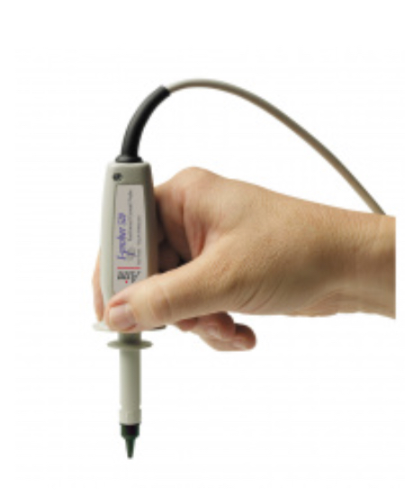
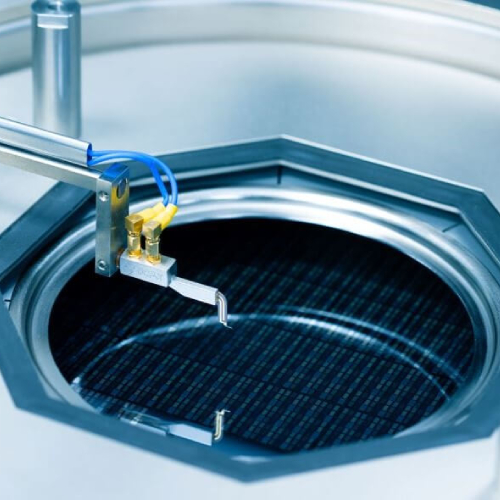
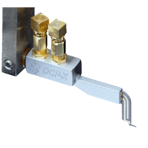
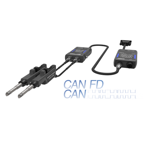
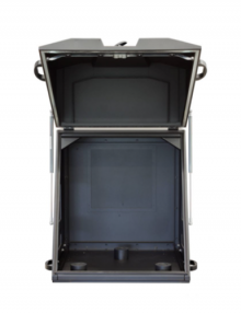
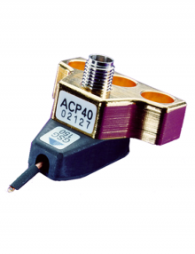
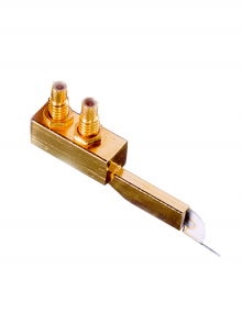
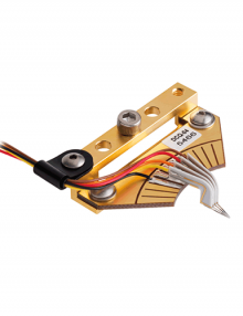
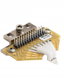
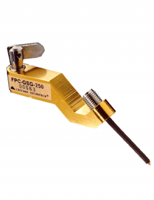
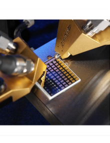
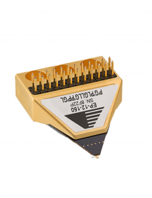
1 800 665 7301 | info@tmetrix.com

Probes

Probes
 
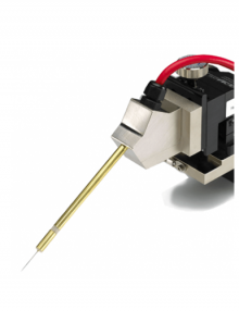
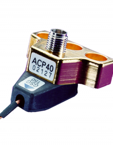
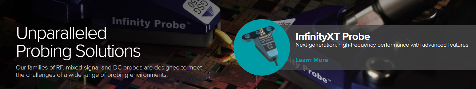
We offer more than 50 analytical probe models for wafer, package, and board level characterization. Our families of RF, mixed-signal and DC probes are designed to meet the challenges of a wide range of probing environments.
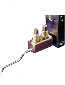
    • Current measurement from insulated probing of conductor
    • Suitable for observation and measurement of current in PCB tracks, component leads and ground planes
    • Wide dynamic range of 10mA to 20A peak to peak
    • Wide bandwidth of DC to 5MHz
    • Low noise figure equivalent to <6mA rms at full B/W
    • Safety rated to 300V Cat II (600V Cat 1)
    • Suitable for connection to any oscilloscope
    • High accuracy general purpose H-field probe
    • Converts to ‘closed magnetic circuit’ current probe


  • The DCP-X probe is designed for engineers and scientists in device characterization, R&D, and testing, offering highly accurate and repeatable on-wafer electrical measurements (IV, CV, LFN). It uses MEMS technology to measure advanced devices (2, 3, 5 nm) on various pad materials, micro-bumps, and pads as small as 20 μm, reducing the need for retesting and cleaning while covering the full thermal range at lower testing costs. Compared to traditional probes, the DCP-X provides 1000x lower contact resistance, minimal skate, and over 500,000 contact cycles, ensuring precise measurements and longer probe life.

    • Highest accuracy with backlash-free positioning
    • Drift-free measurements over temperature and time*
    • Easy, and safe swapping between arms
    • Best signal integrity using optimized probe cabling systems
    • Full thermal capability*
    • Manual or progammable


  • Accurate and precise measurement of device parameters up to 3,000 V

    • Coaxial and triaxial measurements up to 3,000 V
    • High-quality construction with low-noise electrical performance
    • Replaceable probe tips in a variety of tip sizes
    • Temperature range of -55 to 300ºC
    • Triaxial measurement ensures a much better understanding of device leakage in the off state
    • Highly reliable, stable and repeatable measurements
    • Integrally designed as part of a complete measurement solution


  • Delivers superior guarding and shielding

    • High-quality construction with low-noise electrical performance
    • Kelvin version for convenient 4-point measurements
    • Replaceable coaxial probe tips, with choice of tip radii, and full electrical guard to the probe tip
    • SSMC 50 connectors
    • Ultra-low, fA and fF measurements from -65 º C to 150 º C


    • Light-tight version and EMI-shielded version for low noise and light-sensitive measurements
    • Application flexibility, ideal for use in high frequency applications
    • Sized to accommodate thermal chucks, laser cutter, and video equipment on the probe system
    • Suitable for integration with vibration isolating tables


    • Functional temperature range of -263 to +150°C
    • Stainless steel tip material for thermal decoupling
    • Coaxial cable with TCE matched inner and outer conductors
    • Consistent tip geometry even at cryogenic temperatures


  • High-performance DC Parametric Probe

    • Ultra-low, fA-level current and fF-level capacitance measurements from -65 °C to + 300 °C
    • Guarantees fully-guarded measurements to fA and fF levels
    • Individual connectors provide force-sense connection for quasi-Kelvin and CV measurements
    • Allows probing of different pad materials and sizes
    • Fast replacement of worn probes without the need for tools


  • Multi-contact DC Probe with flat tip needles

    • Power bypass inductance: 8 nH
    • Standard DCQ probes have flat tip needles available in nickel-plated tungsten or BeCu with diameters of 0.75 mil, 1.0 mil and 1.5 mil.
    • Supports collinear and non-standard needle configurations
    • Up to 16 DC for standard; maximum of 24 DC for custom
    • Ideal for probing the entire circuit for functional test
    • DC probes can provide power or slow logic to circuit under test


  • Multi-contact DC Probe with full-radius needles

    • Full-radius, nickel-plated tungsten needles
    • Power bypass inductance: 16 nH
    • Supports collinear and non-standard needle configurations
    • Support up to a maximum of 12 ceramic blades DC needles / contacts
    • Ideal for probing the entire circuit for functional test
    • DC probes can provide power or slow logic to circuit under test


  • Rugged, deep reach RF probing for modules and circuit boards

    • DC-40 GHz bandwidth
    • 10 ps rise time
    • Low insertion and return loss
    • 2 mils of tip-to-tip compliance
    • High probing angle and clearance


  • Perfectly matched to the |Z| Probe®

    The CSR family of calibration substrates delivers the highest accuracy available due to the high quality of each substrate. The calibration standards are manufactured using rugged, hard gold, which ensures a long lifetime.


  • Durable multi-contact wafer probe with controlled impedance power bypass technology

    • High performance power bypassing provides low-impedance and resonant-free connections to 20 GHz
    • RF bandwidth to 500 MHz
    • Long probe life: > 250,000 contacts
    • Beryllium-copper tips for gold pads or tungsten for aluminum pads
    • Oscillation-free testing of wide-bandwidth analog circuits
    • Use with ACP series probes to provide functional at-speed testing for known-good-die
    • Mix multiple contact types: Ground, Power (Standard or Eye-Pass), Logic/Signal
    • Low and repeatable contact resistance on aluminum pads ( < 0.25 Ω on Al, < 0.01 Ω on Au)


  • Multiline TRL Substrates for T-Wave Probes

    • Substrate material: High-resistivity silicon
    • Substrate thickness: 275 µm
    • Dielectric constant: 11.8
    • Nominal Z0: 50 Ω


  • Long-lasting, rugged RF and microwave on-wafer probes

    • Unique Air Coplanar tip design with choice of beryllium copper (BeCu) or tungsten tip material
    • DC to 110 GHz models available in single and dual line versions
    • Low insertion and return loss with ultra-low-loss ( -L ) versions
    • Excellent crosstalk characteristics
    • Wide operating temperature -65 ° C to + 200 ° C
    • Wide range of pitches available, from 50 to 1250 µm
    • Individually supported contacts
    • Reduced contact (RC) probe tips for small pads
    • BeCu tip provides rugged, repeatable contact on gold pads