Discount Products: Look through products available for a 25% – 50% discount in 2020. The items provided on a first come, first serve basis.
View Discounted Products
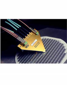
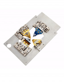
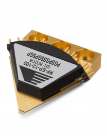
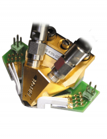
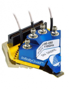
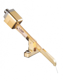
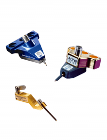
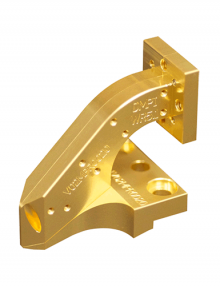
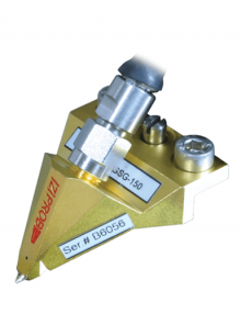
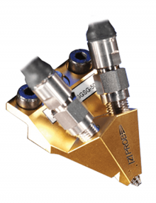
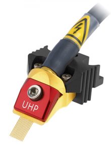
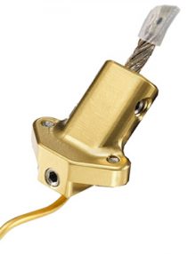
Probes

Probes
 
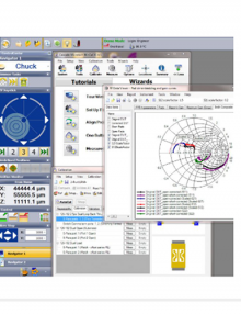
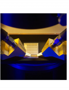
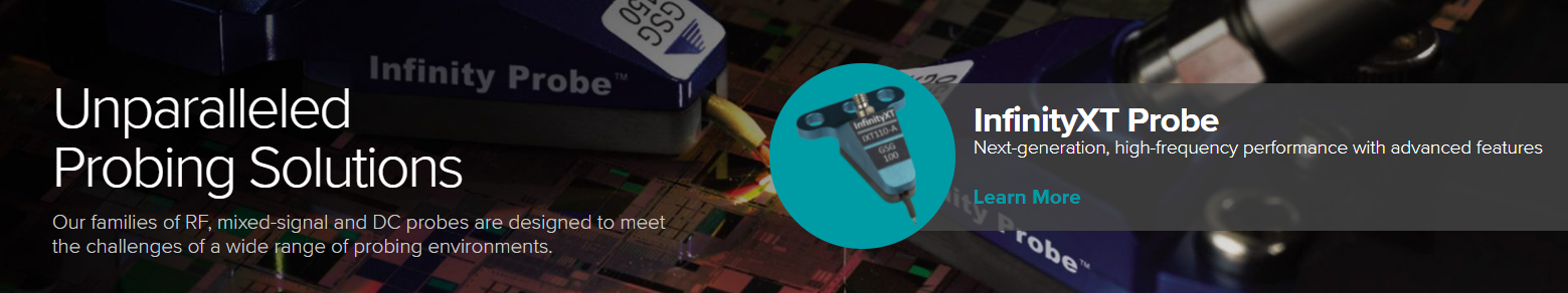
We offer more than 50 analytical probe models for wafer, package, and board level characterization. Our families of RF, mixed-signal and DC probes are designed to meet the challenges of a wide range of probing environments.

Showing 17–30 of 30 results


  • Test Up to 16 RF Signals with One Probe

    • Ideal for multiport RF/Microwave and high-speed digital signal testing
    • Mix DC and RF/Microwave signals on one probe
    • Long lifetime – typically over one million (1,000,000) touchdowns
    • Excellent performance in temperatures ranging from 10 K to 200°C
    • Probe on any pad material with no damage


    REQUEST A QUOTE
  • Cost-effective, versatile probe card solution

    • Accommodates a combination of up to four Cascade Microtech probes
    • Configurable for mixed-signal RF/mmW testing
    • Quick and easy repairs to be performed in the field, by simply replacing individual probes
    • Adaptable to new device layouts by exchanging individual probes


    REQUEST A QUOTE
  • Multicontact Probe for RFIC Engineering Test

    • Up to 12 contacts; any contact can be DC, Power, Logic to 500 MHz,or RF to 20 GHz
    • Online design configuration tool helps you to specify your probe in minutes
    • All designs are fully quadrant compatible
    • Full solution includes probes, calibration substrates, stations, accessories and software
    • Scalable architecture for future needs


    REQUEST A QUOTE
  • HF and DC Signals on One Cost-Effective ProbeWedge

    • Flexibility
      • The ProbeWedge family is compatible with your existing Cascade Microtech’s probing systems
      • Plug and play design provides easy handling and strain relief
      • Ideal probe solution for wafer-level reliability, multi-site tests and DC biasing
    • Cost effectiveness
      • Alternative to inflexible probe cards, ideal for changing demands in R&D
      • All cables can be re-used and additional single cables can be ordered
      • Probe blades can be repaired individually
    • Accuracy
      • Kelvin ProbeWedge is ideal for low-resistance measurements
      • Fully-guarded microstrip blades for low-current measurements down to fA range


    REQUEST A QUOTE
  • A configurable fine-pitch multi-contact RF/mmW probe for mixed-signal probing up to 110 GHz

    • Customizable configuration up to 25 contacts: RF, Eye-Pass power, ground, logic
    • Lithographically-defined tips allow automated over temperature measurement on pads as small as 30 µm x 50 µm
    • Low and repeatable contact resistance on aluminum pads (< 0.05 Ω) ensures accurate results
    • Durable probe structure ensures more than 250,000 contacts
    • Able to measure from -40°C to +125°C without compromising performance or accuracy of specifications


    REQUEST A QUOTE
  • Multi-Configurable Optical Probe for Photonic Device Characterization

    • Flexibility and ease of use
      • Field-replaceable fibers optimized for a variety of applications
      • Wafer mapping capability and visual display of key parameters
    • Accuracy
      • Patented contact protection design ensures fast, accurate, and repeatable measurements at the wafer and substrate level
      • Minimized electrical parasitics for at-speed testing
    • Compatibility
      • Standard FC type fiber-optic connector
      • Compatible with FormFactor probe stations and accessories


    REQUEST A QUOTE
  • Custom configured for your application

    • Choice of Series resistance or Termination (signal line to ground)
    • Use of High Performance RF Resistors
    • Choice of Resistor values available
    • Choice of body styles, Infinity, ACP or FPC


    REQUEST A QUOTE
  • Wafer-level electrical measurement of mmW devices and materials up to 1.1 THz

    • Low insertion loss
    • Low contact resistance
    • 140 GHz – 1.1 THz versions
    • Probe pitch as narrow as 25 μm
    • Lithographically-defined probe tip
    • Nickel contacts


    REQUEST A QUOTE
    • Supports up to 12 VNA ports than can be mapped to four logical ports for calibration
    • Extensive guidance, wizards and management features automate calibration setup, measurement, result data conversion and report creation
    • LRRM-SOLT, multi-line TRL and second-tier calibration methods enable precision and simple multi-port calibrations
    • Automatic load inductance compensation function ensures the most repeatable calibrations
    • Easy to use Probe to ISS/CSR matching tool
    • Additional remoting methods
    • Interface with Velox™ over LAN


    REQUEST A QUOTE
  • Robust RF Test on PCB and Ceramic

    • Replace costly and inflexible test fixtures with easy-to-use probe tips
    • Long lifetime – typically over 1,000,000 contacts
    • GS/SG footprint up to 4 GHz and GSG up to 20 GHz
    • High-power RF test: up to 30 Watts
    • Test at temperatures from -60°C to 200°C


    REQUEST A QUOTE
  • High power, High performance probe

    • High power – 66 W at 2.4 GHz and 43 W at 5 GHz
    • Extremely low insertion loss of ≤ 0.4 dB (typical) up to 40 GHz
    • Excellent contact control and low contact resistance
    • High performance on any pad material (Al or Au)
    • Longest lifetime – typically one million (1,000,000) touchdowns


    REQUEST A QUOTE
  • Excellent Performance – Longest Lifetime

    • Best price per contact – typically over one million (1,000,000) touchdowns
    • RF/Microwave signal is shielded and completely air isolated in the probe body
    • Excellent performance in vacuum environments and temperatures as low as 4 K, or as high as 300°C
    • Highest impedance control with perfectly-symmetrical, MEMS-machined coplanar contact structure
    • Probe on any pad material with minimal damage


    REQUEST A QUOTE
  • Enabling single-contact high-current/high-voltage test

    • Enables coaxial measurements up to 10,000 V and 300 A pulsed (600 A in a parallel configuration) with a single touchdown
    • Even distribution of high current with innovative multi-fingertip design
    • Compatible with Tesla 200/300 mm power device characterization system
    • Reduced measurement time by testing both high-voltage and high-current conditions with a single touchdown
    • Accurate characterization of a wide range of pad sizes and test currents, with minimum pad damage and contact resistance
    • Safe, reliable and repeatable high-current/voltage measurements over a wide temperature range (from -55°C to +300°C)


    REQUEST A QUOTE
  • Test power devices on wafer with high-performance and low-contact resistance on smaller pads

    • Minimal contact resistance at the pad-tip junction to reduce heating during measurements, with fewer probe marks
    • Measure devices on wafer at high-current conditions over a wide temperature range (-55°C to 300°C)
    • Small scrub minimizes damage on Al pad
    • Small footprint – tip for small pad probing down to 1 mm x 1 mm pad


    REQUEST A QUOTE

Showing 17–30 of 30 results

Filters


Suppliers

Latest News