1 800 665 7301 | info@tmetrix.com

Uncategorized


  • The EME Guard Plus is a lightweight and robust personal protection monitor designed to ensure the safety of workers operating near electromagnetic field (EMF) emitters such as antennas, radars, and base stations. With a frequency range of 1 MHz to 40 GHz, this device continuously monitors and records EMF exposure levels while providing immediate audio, visual, and vibrating alerts when exposure exceeds predefined safety thresholds. Customizable alarm settings and a triaxial isotropic probe ensure accurate and reliable measurements.


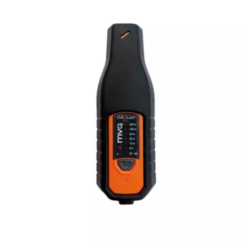
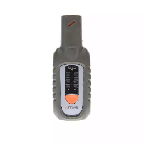
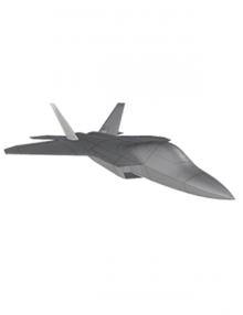
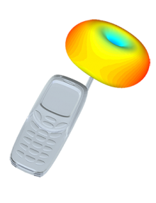
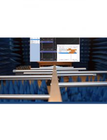
  • The EME Guard XS Radar is a state-of-the-art RF safety monitor, specifically designed for workers operating near radar transmitters and antennas. With its isotropic tri-axis E-field sensors, this compact device provides continuous EMF monitoring over a frequency range of 1 MHz to 40 GHz, including short pulsed signal detection. Equipped with audio and visual alarms, it alerts users instantly when EMF exposure exceeds predefined safety thresholds, creating a safer working environment for military, aviation, and telecom personnel.


  • PureLine 3 Technology

    First automated probe station to achieve -190dB spectral noise*

    Plug In and Go

    Integrated TestCell Power Management provides fully managed and filtered AC power to the entire system, prober and instruments

    Autonomous 24/7 Operation

    Up to 4x faster flicker noise thermal testing on 30 μm pads

    Reduce Setup Time and Costs
    Exclusive low noise site survey, and system verification services


    • Quick and easy probe tip navigation
    • Maximizes field-of-view
    • High magnification
    • Shadow-free view of the corresponding features
    • Automatically configure and optimize performance
    • cTUVus certified and CE
    • Compatible with TopHat for perfect shielding
    • 24/7 operating, Increased MTBF
    • Stops all system motion and warns of unobserved contact


    • Comprehensive,
    • Turn-key Integrated Measurement System (IMS)
    • with Keysight PNA for On-wafer R&D Measurements
    • from RF to millimeter wave to Terahertz


  • Accurate and precise measurement of device parameters up to 3,000 V

    • Coaxial and triaxial measurements up to 3,000 V
    • High-quality construction with low-noise electrical performance
    • Replaceable probe tips in a variety of tip sizes
    • Temperature range of -55 to 300ºC
    • Triaxial measurement ensures a much better understanding of device leakage in the off state
    • Highly reliable, stable and repeatable measurements
    • Integrally designed as part of a complete measurement solution


  • Delivers superior guarding and shielding

    • High-quality construction with low-noise electrical performance
    • Kelvin version for convenient 4-point measurements
    • Replaceable coaxial probe tips, with choice of tip radii, and full electrical guard to the probe tip
    • SSMC 50 connectors
    • Ultra-low, fA and fF measurements from -65 º C to 150 º C


  • High-performance DC Parametric Probe

    • Ultra-low, fA-level current and fF-level capacitance measurements from -65 °C to + 300 °C
    • Guarantees fully-guarded measurements to fA and fF levels
    • Individual connectors provide force-sense connection for quasi-Kelvin and CV measurements
    • Allows probing of different pad materials and sizes
    • Fast replacement of worn probes without the need for tools


  • Multi-contact DC Probe with flat tip needles

    • Power bypass inductance: 8 nH
    • Standard DCQ probes have flat tip needles available in nickel-plated tungsten or BeCu with diameters of 0.75 mil, 1.0 mil and 1.5 mil.
    • Supports collinear and non-standard needle configurations
    • Up to 16 DC for standard; maximum of 24 DC for custom
    • Ideal for probing the entire circuit for functional test
    • DC probes can provide power or slow logic to circuit under test


  • Multi-contact DC Probe with full-radius needles

    • Full-radius, nickel-plated tungsten needles
    • Power bypass inductance: 16 nH
    • Supports collinear and non-standard needle configurations
    • Support up to a maximum of 12 ceramic blades DC needles / contacts
    • Ideal for probing the entire circuit for functional test
    • DC probes can provide power or slow logic to circuit under test


  • Rugged, deep reach RF probing for modules and circuit boards

    • DC-40 GHz bandwidth
    • 10 ps rise time
    • Low insertion and return loss
    • 2 mils of tip-to-tip compliance
    • High probing angle and clearance


    • SlimVue Microscope
      • Combined eye-pieces and CCD camera mount
      • 3x zoom and quick lens exchange
      • Quick lens exchange
      • 1 um optical resolution
      • Minimized scope footprin
    • Application Specific Sigma Kits
      • Optical feedback on platen position (gauge)
      • Adaptable to any mmW/sub-THz applications
      • Seamless integration with any mmW modules and tuners
      • Fast mounting and setup change
    • THz measurement capability
      • Rock-solid mechanical design
      • Submicron stage accuracy
      • Optical feedback on platen and probe position (gauge)
      • Motorized positioner


  • Durable multi-contact wafer probe with controlled impedance power bypass technology

    • High performance power bypassing provides low-impedance and resonant-free connections to 20 GHz
    • RF bandwidth to 500 MHz
    • Long probe life: > 250,000 contacts
    • Beryllium-copper tips for gold pads or tungsten for aluminum pads
    • Oscillation-free testing of wide-bandwidth analog circuits
    • Use with ACP series probes to provide functional at-speed testing for known-good-die
    • Mix multiple contact types: Ground, Power (Standard or Eye-Pass), Logic/Signal
    • Low and repeatable contact resistance on aluminum pads ( < 0.25 Ω on Al, < 0.01 Ω on Au)


    • Three Probe Technologies
      • nfinity Probe: best for Al (Si)
      • ACP Probe: best for AU (III-Vs)
      • |Z| Probe: robust solution (long lifetime)
    • Precise Contact Solution
      •  Precision probe alignment
      • Consistent contact force and overtravel
      • Stable contact performance
    • WinCal XE Calibration Software
      • Exclusive 1-, 2-, 3-, and 4-port on-wafer calibration algorithms
      • Automated calibration monitoring
      • Unique measurement & analysis methods


  • 200 mm semi-/ fully-automated production probe system

    • Up to 20 dies/sec (70,000 dies/hour) with MultiDie Testing technology
    • Faster time to data
    • Highest Z-axis resolution of any production prober
    • Highest Z-axis resolution of any production prober
    • Interfaces to all major analysis instrumentation, optics software and testers
    • Backside instrumentation, e.g.: Integrating Sphere, Fiber setup, Pressure Module
    • Highly accurate light measurement


  • Long-lasting, rugged RF and microwave on-wafer probes

    • Unique Air Coplanar tip design with choice of beryllium copper (BeCu) or tungsten tip material
    • DC to 110 GHz models available in single and dual line versions
    • Low insertion and return loss with ultra-low-loss ( -L ) versions
    • Excellent crosstalk characteristics
    • Wide operating temperature -65 ° C to + 200 ° C
    • Wide range of pitches available, from 50 to 1250 µm
    • Individually supported contacts
    • Reduced contact (RC) probe tips for small pads
    • BeCu tip provides rugged, repeatable contact on gold pads