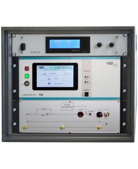
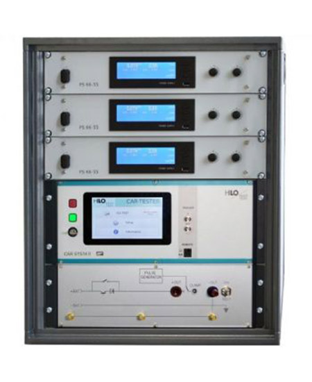
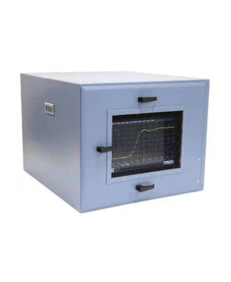
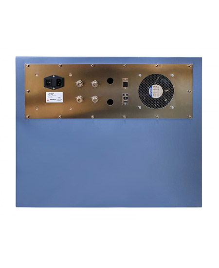
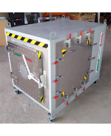
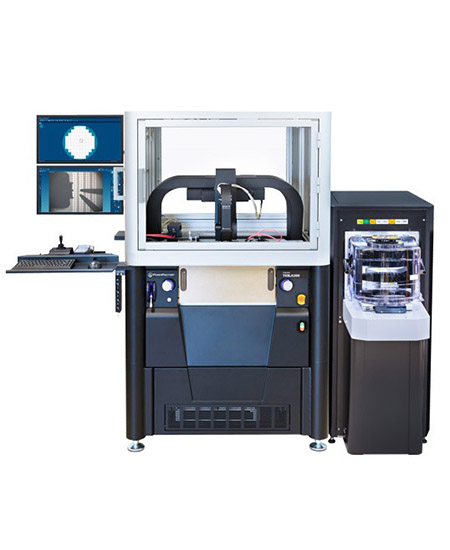
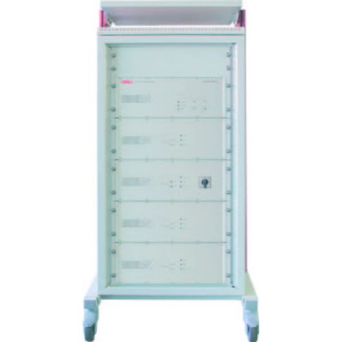
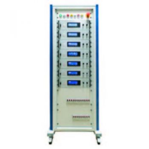
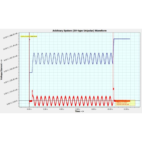
1 800 665 7301 | info@tmetrix.com

    • On-wafer power device characterization up to 10,000 V DC / 600 A
    • Reduced probe and device destruction at high currents up to 20 A DC and 300 A pulse
    • Prevent thin wafers from curling and breaking
    • Accurate Rds(on) measurement at high current
    • Accurate UIS measurements at high temperature
    • Roll-out stage for full wafer access and easy wafer loading/unloading
    • Seamless integration between Velox and analyzers/measurement software
    • High-throughput wafer autoloading (standard, thinned, warped, TAIKO)
    • Easy on-screen navigation, wafer mapping, and operation of accessories with Velox
  • Enabling single-contact high-current/high-voltage test

    • Enables coaxial measurements up to 10,000 V and 300 A pulsed (600 A in a parallel configuration) with a single touchdown
    • Even distribution of high current with innovative multi-fingertip design
    • Compatible with Tesla 200/300 mm power device characterization system
    • Reduced measurement time by testing both high-voltage and high-current conditions with a single touchdown
    • Accurate characterization of a wide range of pad sizes and test currents, with minimum pad damage and contact resistance
    • Safe, reliable and repeatable high-current/voltage measurements over a wide temperature range (from -55°C to +300°C)