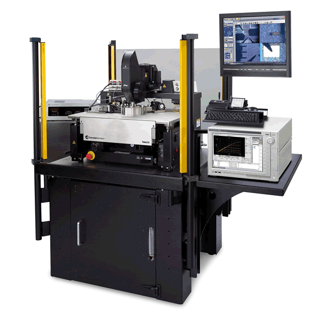
Tesla T200 Overview
The Tesla T200 200mm semi-automatic power device characterization system provides a complete on-wafer solution for over-temperature, low-contact resistance measurements of power semiconductors up to 3,000 V (triax)/10,000 V (coax) and 200 A (pulsed)/10 A (DC). It does this while providing a low-noise, fully guarded and shielded test environment, as well as a certified safety interlock system integrated with an ergonomic clear enclosure or infrared laser light curtain.
Tesla T200 Key Features
|
|
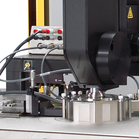
Seamless integration
- Convenient instrument connection kits
- Seamless integration between Velox and analyzers/measurement software
- Easy and safe system integration with Keysight and Keithley power device analyzers
|
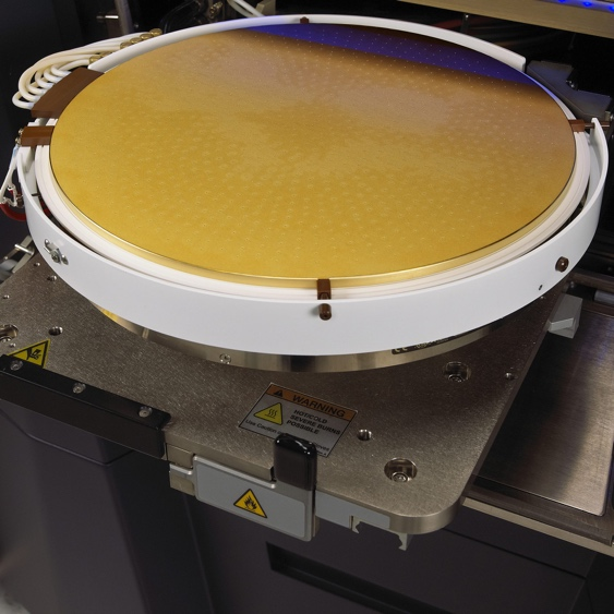
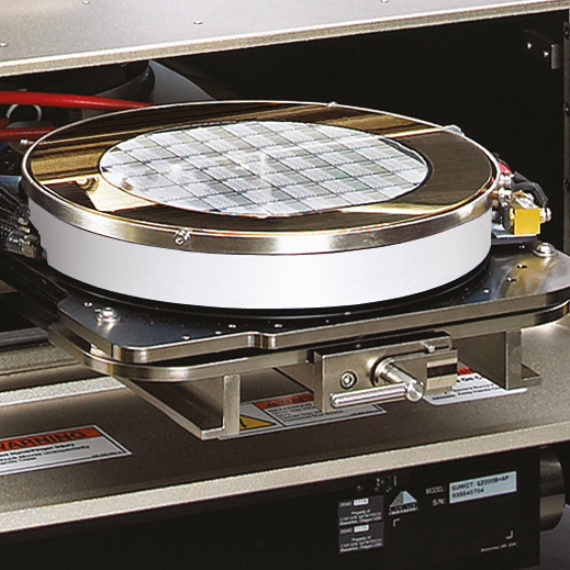
MicroVac™ chuck
- 495 uniformly distributed vacuum micro-holes
- Gold-plated, high-power chuck surface
- Thin-wafer handling capability
- Low electrical and thermal contact resistance across the entire wafer
- Prevents thin wafers from curling and breaking
|
|
|
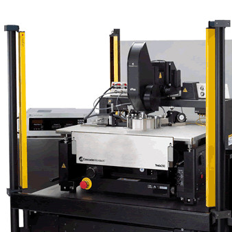
Safety
- Regulatory-certified probing environment
- Safety interlock system with clear enclosure or light curtain
- Fully guarded and shielded test environment
- Operator safety during measurements
- Protects device and instrumentation from high-voltage discharge
|
Ease of use
- Roll-out stage
- Full wafer access and easy wafter loading/unloading
|
|
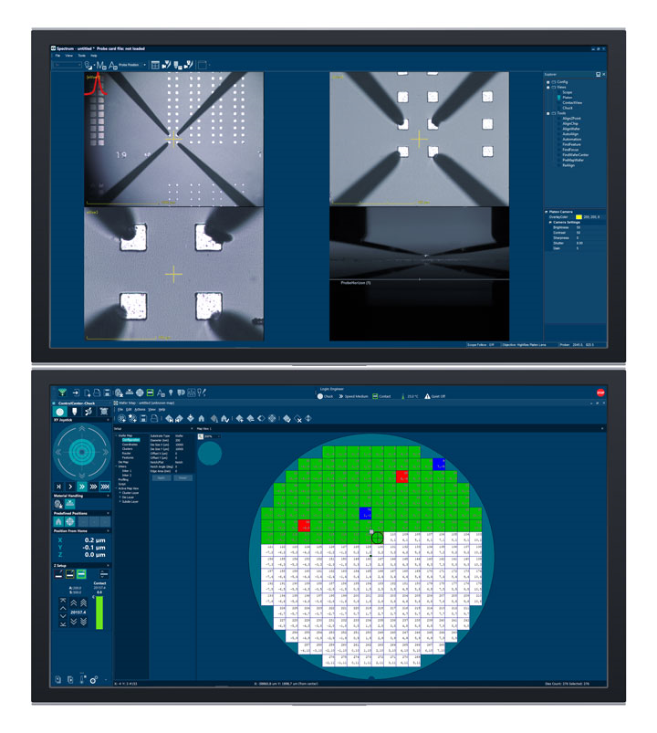 |
Velox probe station control software
- User-centered design minimizes training costs, enhances efficiency
- Windows 10 compatibility enables highest performance and safe operation with state-of-the art software
- Comprehensive alignment functions
- Simplified operation for inexperienced users
|