Description
|Z| Probe® Power Overview
The demand for access to rich content anywhere in the world is driving the growth of wireless transmission of information. This increases the need for RF power devices in wireless systems and new technologies such as GaN and SiC. This in turn necessitates the characterization of these new technologies at wafer-level, which significantly reduces the time needed to develop new models. These models are used in new device designs, which are then further implemented in wireless transmission systems (base stations, satellites, etc.) to meet the demands of the content-hungry consumer.
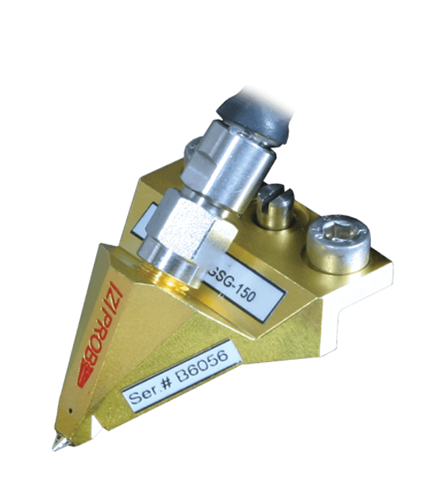
To provide highly accurate characterization of RF power devices at wafer level, the |Z| Probe® Power, based off proven |Z| Probe technology, handles high power at high frequencies (up to 40 GHz). The |Z| Probe Power provides excellent contact repeatability and extremely low contact resistance to deliver accurate results in load-pull measurement setups, which are typical for characterizing RF power devices.
Since insertion loss must be kept low in load-pull and noise-parameter measurements to secure a high reflection coefficient (Γ), |Z| Probe Power has been designed to provide an extremely low insertion loss. This means you get more accurate measurements especially at non-50 Ω impedances.
|Z| Probe® Power Key Features
- High power – 66 W at 2.4 GHz and 43 W at 5 GHz
- Extremely low insertion loss of ≤ 0.4 dB (typical) up to 40 GHz
- Excellent contact control and low contact resistance
- High performance on any pad material (Al or Au)
- Longest lifetime – typically one million (1,000,000) touchdowns

